PCB Layout
Expert Design for Success
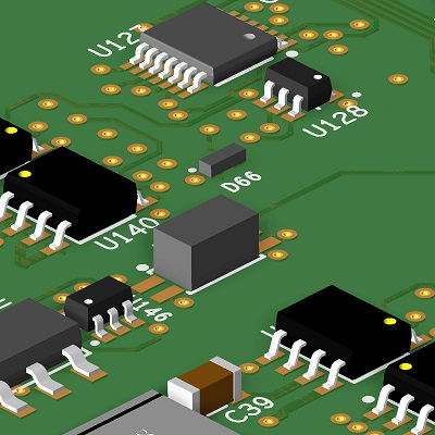
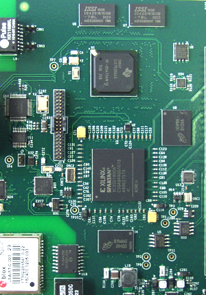
Our expert PCB Layout team can handle your most challenging design requirements. We deliver quality printed circuit board layouts with emphasis on Design for Manufacturability (DFM) and Constraint Driven Design. Our past projects include a wide range of technologies covering High-Speed FPGA, DDR2/DDR3 memory, RF applications, SMPS (Switch Mode Power Supply) & much more.
Constraint Driven PCB Design
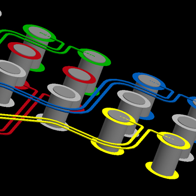
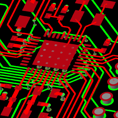
Constraint driven design methods are used to meet the most rigorous project requirements including matched length traces, differential pairs, controlled impedance and RF signals. Our team has a wealth of experience covering High-density FPGA/DDRx digital designs, RF modules (Bluetooth, GPS), Switch-mode power supplies and more.
Optimization
Manufacturing, Engineering & Layout under one roof
Having PCB design and assembly under the same roof has allowed us to develop a rigorous set of design constraints & optimizations aimed at manufacturability and cost effectiveness. Our internal Design For Manufacturability (DFM) methods target PCB fabrication issues, solderability, documentation, production yield and overall cost.
Flexibility
Your Partner in Design
As the customer, you decide how much or how little you are involved in the PCB Design phase. We offer a flexible service based on your project and your schedule. Our team can manage your project from start to finish with minimal input from you. If you prefer complete control over component placement and routing, we can contribute advice and input concerning sound design practices, signal integrity and manufacturability throughout the design phase.
Certified Expertise
Your PCB Layout project will be handled by an Advanced Certified Interconnect Designer (CID+) certified by the IPC Designers Council.